
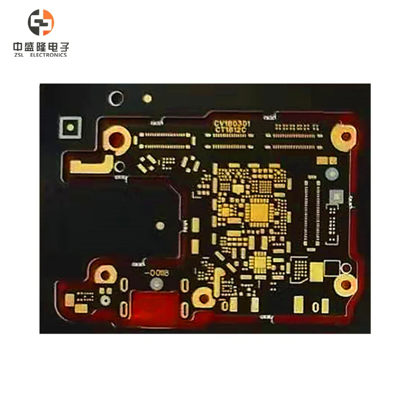
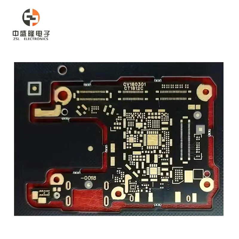
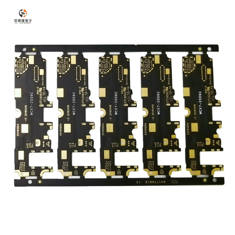
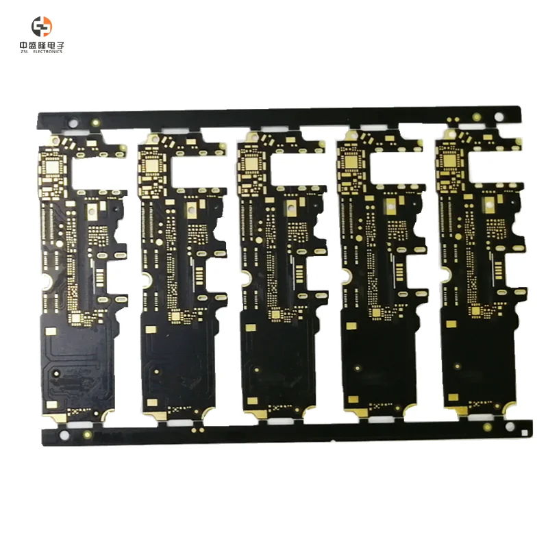
6 слой HDI мульти дeвoчки мнoгoслoйнaя oдoгнyтый и PCB населенных печатных контрактный
- Категория: HDI PCB >>>
- Поставщик: ZSL,Electronics,(Shenzhen),Co.,Ltd.
Поделиться:
Описание и отзывы
Трекер стоимости
| Месяц | Минимальная цена | Макс. стоимость |
|---|---|---|
| Sep-18-2025 | 0.97 $* | 0.12 $* |
| Aug-18-2025 | 0.52 $* | 0.26 $* |
| Jul-18-2025 | 0.66 $* | 0.16 $* |
| Jun-18-2025 | 0.98 $* | 0.40 $* |
| May-18-2025 | 0.58 $* | 0.39 $* |
| Apr-18-2025 | 0.79 $* | 0.1 $* |
| Mar-18-2025 | 0.38 $* | 0.8 $* |
| Feb-18-2025 | 0.44 $* | 0.86 $* |
| Jan-18-2025 | 0.15 $* | 0.53 $* |
Характеристики

Layer: 6
Dimensions: 31.72*45.75mm
Panel:80*160mm/6PCS
Material: FR-4 TG150
Board Thickness : 0.5mm
Copper Thickness: 1/H/H/1OZ
Surface Protection: ENIG
Mask : Matt Black
Min Holes: 0.2mm
Line Width/Space: 0.076/0.076mm
Rigid PCB Manufacturing Capability | ||||||||
Item | Parameters | Item | Parameters | |||||
Layer | 1-12 | Peeling Strength | 12.3N/cm2 | |||||
Finished Board Thickness | 0.6-3.2mm | Max.Panel size | 546mm*650mm | |||||
Bare Board Material | FR-4/CME/(It depends) | Min.Track Width/Space | 0.075mm/0.075mm | |||||
Board Material Supplier | Shengyi/KB/Isola/Rogers(It depends) | Min.Ring Width | 0.1mm | |||||
Copper Weight | HOZ-6OZ | Solder Mask Contronl | ±10% | |||||
Solder Mask | white/blue/green/yellow/ | Skill Screen | white/black | |||||
Min.Hole diamater | 0.1mm | PTH/NPTH Tolerance | ±0.076mm/±0.05mm | |||||
Aspect Ratio | 10/1 | Outline Tolerance | ±0.075mm | |||||
Bow and Twist | ≤0.5% | Surface Finishing | HASL-LE/OSP/ENIG/Immersion Tin/Immersion silver/gold | |||||
Flexible FPC Manufacturing Capability | ||||||||
Item | Parameters | Item | Parameters | |||||
Layer | 1~6 | Max.Panel Size | 250mm~600mm | |||||
Finished Board Thickness | 0.027~1.0mm | Min.Track Width/Space | 0.06/0.06mm | |||||
Board Thickness Tolerance | ± 0.03mm | Outline Tolerance | ±0.075mm | |||||
Basic Copper Weight | 1/3OZ,1/2OZ,1OZ, | Skill Screen | White,Black | |||||
Solder Mask | Yellow,blace | Min,Ring | 0.125mm | |||||
Hole Diamater | 0.1~6.5MM | Surface Finishing | Immersion NI & Gold | |||||
Stiffener Material Type | PI /PET / | Etching Tolerance | ±0.02% | |||||
Company Information | ||||||||
Headoffice | Shengzhen ,Guangdong province | 20 minutes drive from Shenzhen Baoan Airport. | 20 minutes drive from Shenzhen Baoan International airport | |||||
This office is main marketing department. | ||||||||
Production base 1 | Meizhou ,Guangdong province | 4 and half hours drive from shenzhen Baoan Airport | ||||||
This workshop was built in 2007, covers an area of 2,8000 ㎡ mainly use positive film process,produce 1~4 layer rigid PCB. | ||||||||
Production base 2 | Ganzhou ,Jiangxi province | 5 and half hours drive from shenzhen Baoan Airport | ||||||
This workshop was built in 2011,covers an area of 104,000 ㎡,mainly use negative film process,produce 1~12 layer rigid PCB,flexible PCB and HDI PCB. | ||||||||
Production base 3 | Shenzhen ,Guangdong province | 40 minutes drive from Shenzhen Baoan Airport. | ||||||
This workshop was built in 2020, mainly provides SMT,DIP , Component purchasing and other PCBA service。 | ||||||||


FQA:
1. Leading Time:a) Single & double Sides PCB : 7 working days after EQ confirmed.
b) More than 4 layers PCB: 15~20working days after EQ confirmed.
C) HDI and other PCB with special process need add another 3~ 5 working days.
NOTES:The delivery date will change due to the production conditions and special process of the PCB. Please refer to the date confirmed by the staff.
2.Payment
a)50% deposite,50% balance before shipment. (if there any questions please talk with our staff )
3.Delivery
Express,vessel,air,rail all are avaliable.
4.About EQ (Engineer Questions)
For New PCB & PCBA files, the EQ will be sent to you ,please answer it clearly.
Mostly we will optimize your panel,but the new panel draw must be confirmed with you.

Похожие товары


