
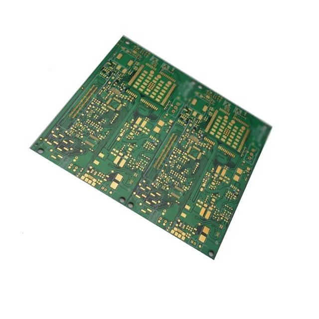
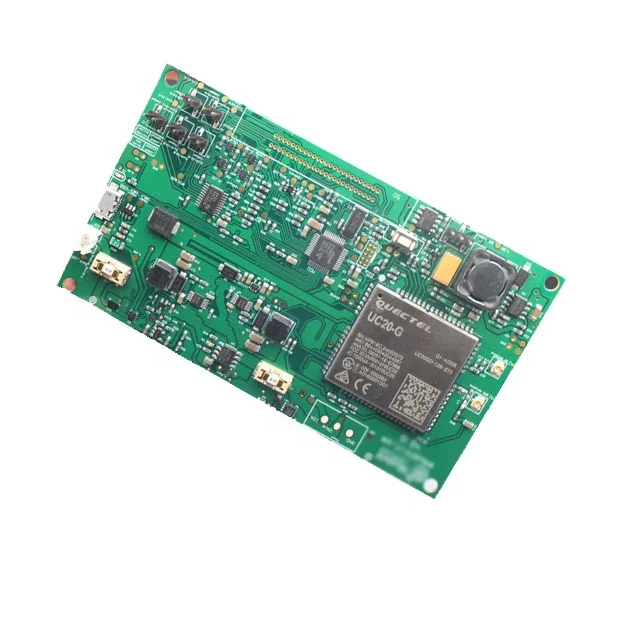
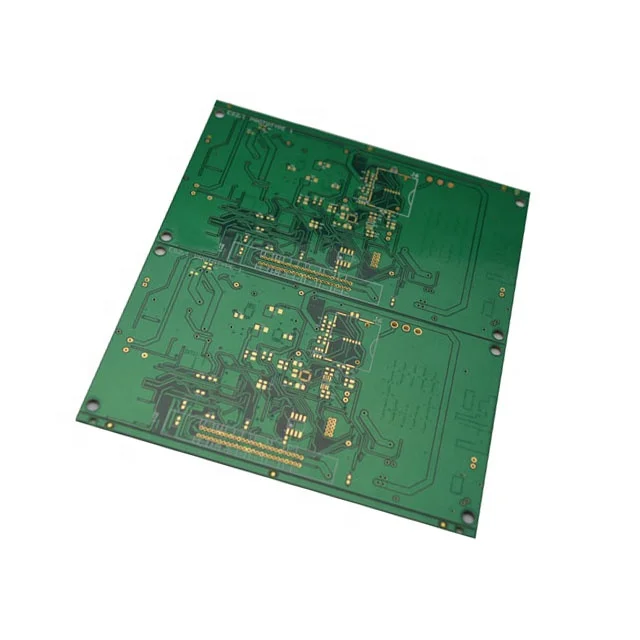
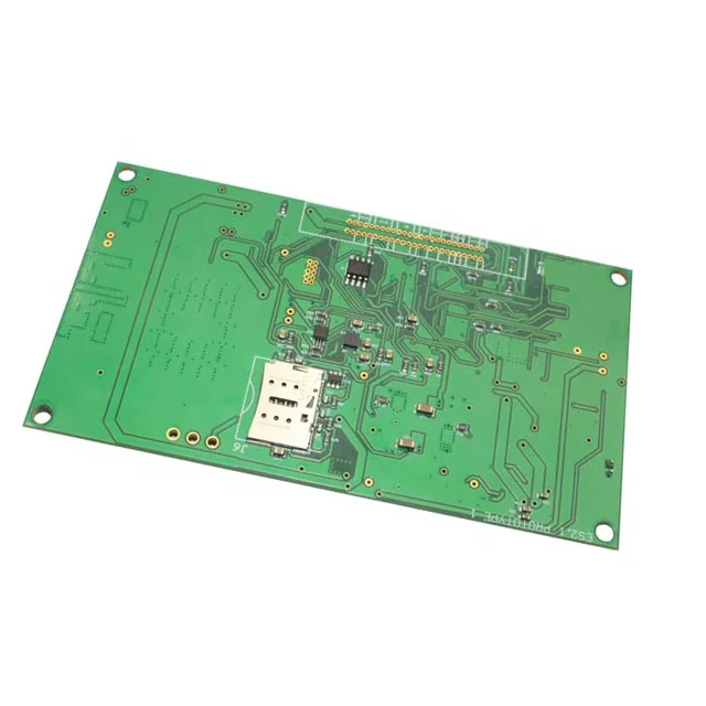
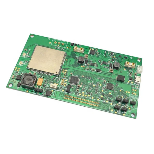
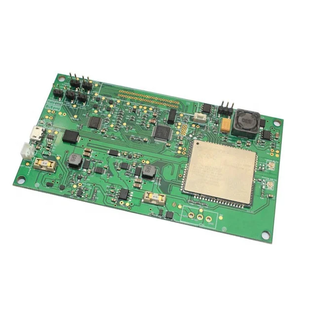
Электронная печатная плата
- Категория: Multilayer PCB >>>
- Поставщик: Shenzhen,Moko,Technology,Ltd.
Поделиться:
Описание и отзывы
Трекер стоимости
| Месяц | Минимальная цена | Макс. стоимость |
|---|---|---|
| Aug-15-2025 | 1.74 $* | 1.88 $* |
| Jul-15-2025 | 1.82 $* | 1.87 $* |
| Jun-15-2025 | 1.39 $* | 1.56 $* |
| May-15-2025 | 1.2 $* | 1.39 $* |
| Apr-15-2025 | 1.76 $* | 1.24 $* |
| Mar-15-2025 | 1.26 $* | 1.73 $* |
| Feb-15-2025 | 1.98 $* | 1.97 $* |
| Jan-15-2025 | 1.93 $* | 1.39 $* |
Характеристики
Our Service
Schematic Capture
Advanced verification features.
Convert schematic to PCB
PCB Layout
High-speed and differential signals, 3D preview, STEP export, Gerber and ODB++ manufacturing output.
3D Modeling
Convert schematic to PCBReal-time 3D PCB preview on any stage of development.

* Professional R&D teams with 40+ engineers.
* 17 Years dlectronic ODM/ODM experience
* 17 Years dlectronic ODM/ODM experience
* 8 SMT , 4 DIP production lines, 8000㎡
Product Description
Design Software :
We specialize in Altium Designer software but have the ability to complete your schematic capture and PCB layout in several different software packages including:
* Altium Designer
* Cadence OrCAD/Allegro
* Legacy PCAD
* Eagle (Altium Conversion)
* Protel
Files needed
Schematic(DSN or powerlogic), netlist, package, structure chart(DXF), Components file, layout requirements etc.
Layout file output
PCB original file, gerber file, pick and place file, framed stencil file and structure file etc.
PCB LAYOUT CAPACITIES | Reach to | ||||||
The max. number of layers | 40 Layers | ||||||
The max. number of pins | 60000 | ||||||
The min. spacing of BGA | 0.2 mm | ||||||
The highest speed of signal | 12G (differential signal) | ||||||
The min. trace width | 2mil (HDI) | ||||||
The min. trace spacing | 2mil (HDI) | ||||||
The max. number of BGA-PIN | 2500 | ||||||
The highest price of HDI | connected with any layers (ELIC) | ||||||
Production Flow
Schematic Capture Process


Visual and Logical Structure
Multi-Level Hierarchy
Electrical Rule Check
PCB Layout Process


Placement Features
Manual Routing
High-Speed Autorouter


High-speed and Differential Signaling
Advanced Verification Features
3D PCB Preview & STEP Export
Company Introduction
Founded in the year 2006,located in Shenzhen, as a professional EMS/OEM Manufacturer in PCB / PCBA.
MOKO covers an area of more than 8,000 square meters, and has over 250 employees, among them, there’re 70 engineers for R&D team and 45 overseas sales for business team.
We have got the ISO9001:2015, ROHS certifications, and UL listed (File Number: E501497 & E499341). We can offer all kinds of services including PCB manufacturing and PCB assembly, sample orders and batch orders. For PCB assembly, utilizing 5 high-speed SMT PCBA lines from Yamaha and Sony, to meet our customers’ need. Now our PCB daily capacity reaches 1000 square meters, and PCB assembly can reach 100,000,000 units per month.
Our ODM & OEM solution offers a range of IoT products for the global smart device market.


R&D Products
Bluetooth Module
Here you can select the right Bluetooth LE(BLE/BTLE) module or Bluetooth 4 module for your project from a range of qualified and certified modules based on Nordic nRF52832, nRF51822, TI CC2541/2540 (HM10/11) CSR8635 chips.
Bluetooth Beacon
You can choose low energy nRF52 bluetooth beacon & gateway for the application like asset tracking, indoor positioning, proximity marketing.
With temperature ,accelerometer ,light sensor and other sensors can be added.
IoT Smart Plug Socket
•Quality Smart Plug Under Your Brand Name and Logo
• Hardware R&D and Manufacturing Capabilities
• Firmware and Software Support: Android & iOS SDK For Your Software Developing, With/without Your Brand Logo.
• Hardware R&D and Manufacturing Capabilities
• Firmware and Software Support: Android & iOS SDK For Your Software Developing, With/without Your Brand Logo.
Certificate
* Factory certificated by ISO9001.
* Product certificated with CE, Rohs.
* Alibaba Golden supplier
* Product certificated with CE, Rohs.
* Alibaba Golden supplier

Packing&Shipping

FAQ
Q: What files do you use in PCBA fabrication?
A: Gerber or Eagle, BOM listing, PNP and Components Position
Q:Is it possible you could offer sample?
A: Yes, we can custom you sample to test before mass production
Q: When will I get the quotation after sent Gerber, BOM and test procedure?
A: Within 6 hours for PCB quotation and around 24 hours for PCBA quotation.
Q: How can I know the process of my PCBA production?
A: 7-10 days for PCB production and components purchasing, and 10 days for PCB assembly and Testing
Q: How can I make sure the quality of my PCBAs?
A: We ensure that each piece of PCBA products work well before shipping. We'll test all of them according to your test procedure.
Also if there are any defect items during the shipping, we also can be free to repair for you.


