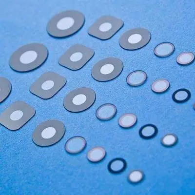


HVPE Вафля из нитрида галлия Индивидуальный размер отдельно стоящий GaN однокристальный
- Категория: Полупроводники >>>
- Поставщик: Shanghai,Clirik,Machinery,Co.,Ltd.
Поделиться:
Описание и отзывы
Трекер стоимости
| Месяц | Минимальная цена | Макс. стоимость |
|---|---|---|
| Sep-17-2025 | 0.98 $* | 0.93 $* |
| Aug-17-2025 | 0.91 $* | 0.63 $* |
| Jul-17-2025 | 0.56 $* | 0.13 $* |
| Jun-17-2025 | 0.21 $* | 0.28 $* |
| May-17-2025 | 0.48 $* | 0.45 $* |
| Apr-17-2025 | 0.24 $* | 0.85 $* |
| Mar-17-2025 | 0.25 $* | 0.62 $* |
| Feb-17-2025 | 0.21 $* | 0.93 $* |
| Jan-17-2025 | 0.2 $* | 0.44 $* |
Характеристики
Product Description
HVPE Gallium Nitride Wafer Customized Size Free - Standing GaN Single Crystal Material

| Product | Gallium nitride (GaN) substrates | ||||||||||||||
| Product Description: | Saphhire GaN template is presented Epitxial hydride vapor phase epitaxy (HVPE) method. In the HVPE process, the acid produced by the reaction GaCl, which is in turn reacted with ammonia to produce gallium nitride melt. Epitaxial GaN template is a cost-effective way to replace gallium nitride single crystal substrate. | ||||||||||||||
| Technical parameters: |
| ||||||||||||||
| Specifications: |
GaN epitaxial film (C Plane), N-type, 2 "* 30 microns, sapphire; GaN epitaxial film (C Plane), N-type, 2 "* 5 microns sapphire; GaN epitaxial film (R Plane), N-type, 2 "* 5 microns sapphire; GaN epitaxial film (M Plane), N-type, 2 "* 5 microns sapphire. AL2O3 + GaN film (N-type doped Si); AL2O3 + GaN film (P-type doped Mg) Note: according to customer demand special plug orientation and size. | ||||||||||||||
| Standard Packaging: | 1000 clean room, 100 clean bag or single box packaging |

Application of HVPE Gallium Nitride Wafer Customized Size Free - Standing GaN Single Crystal Material
GaN can be used in many areas such as LED display, High-energy Detection and Imaging,
Laser Projection Display, Power Device, etc.
- Laser Projection Display, Power Device, etc.
- Date storage
- Energy-efficient lighting
- Full color fla display
- Laser Projecttions
- High- Efficiency Electronic devices
- High- Frequency Microwave Devices
- High-energy Detection and imagine
- New energy solor hydrogen technology
- Environment Detection and biological medicine
- Light source terahertz band

Specifications of HVPE Gallium Nitride Wafer Customized Size Free - Standing GaN Single Crystal Material
| Non-Polar Freestanding GaN Substrates(a-plane and m-plane) | ||
| Item | GaN-FS-a | GaN-FS-m |
| Dimensions | 5.0mm×5.5mm | |
| 5.0mm×10.0mm | ||
| 5.0mm×20.0mm | ||
| Customized Size | ||
| Thickness | 330 ± 25 µm | |
| Orientation | a-plane ± 1° | m-plane ± 1° |
| TTV | ≤15 µm | |
| BOW | ≤20 µm | |
| Conduction Type | N-type | |
| Resistivity(300K) | < 0.5 Ω·cm | |
| Dislocation Density | Less than 5x106 cm-2 | |
| Useable Surface Area | > 90% | |
| Polishing | Front Surface: Ra < 0.2nm. Epi-ready polished | |
| Back Surface: Fine ground | ||
| Package | Packaged in a class 100 clean room environment, in single wafer containers, under a nitrogen atmosphere. | |
FAQ
Q: What's the way of shipping and cost?
A:(1) We accept DHL, Fedex, EMS by FOB.
Q: How to pay?
A: T/T, IN advance
Q: What's your MOQ?
A: (1) For inventory, the MOQ is 30g.
(2) For customized commen products, the MOQ is 50g
Q: What's the delivery time?
A: (1) For the standard products
For inventory: the delivery is 5 workdays after you place the order.
For customized products: the delivery is 2 -4 weeks after you order contact.
Похожие товары