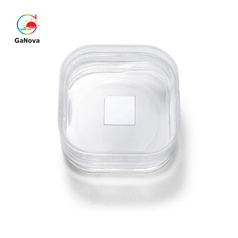
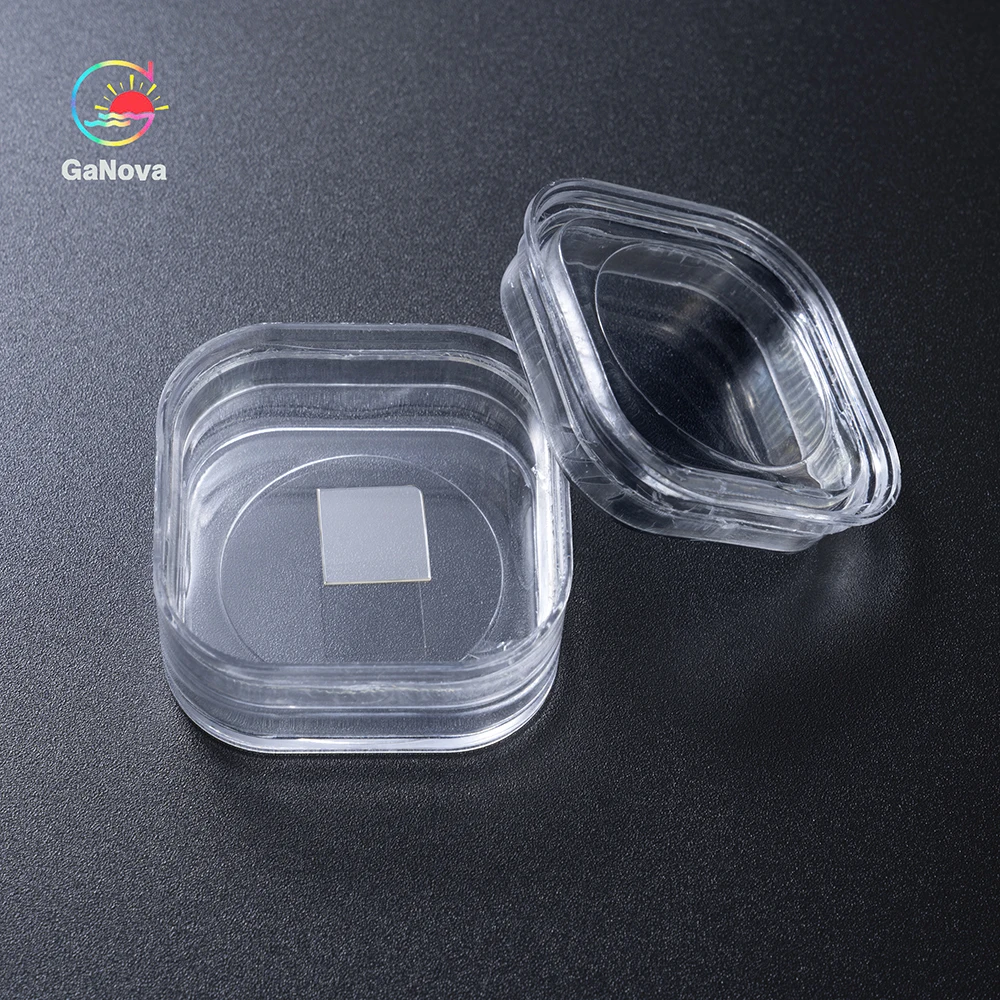
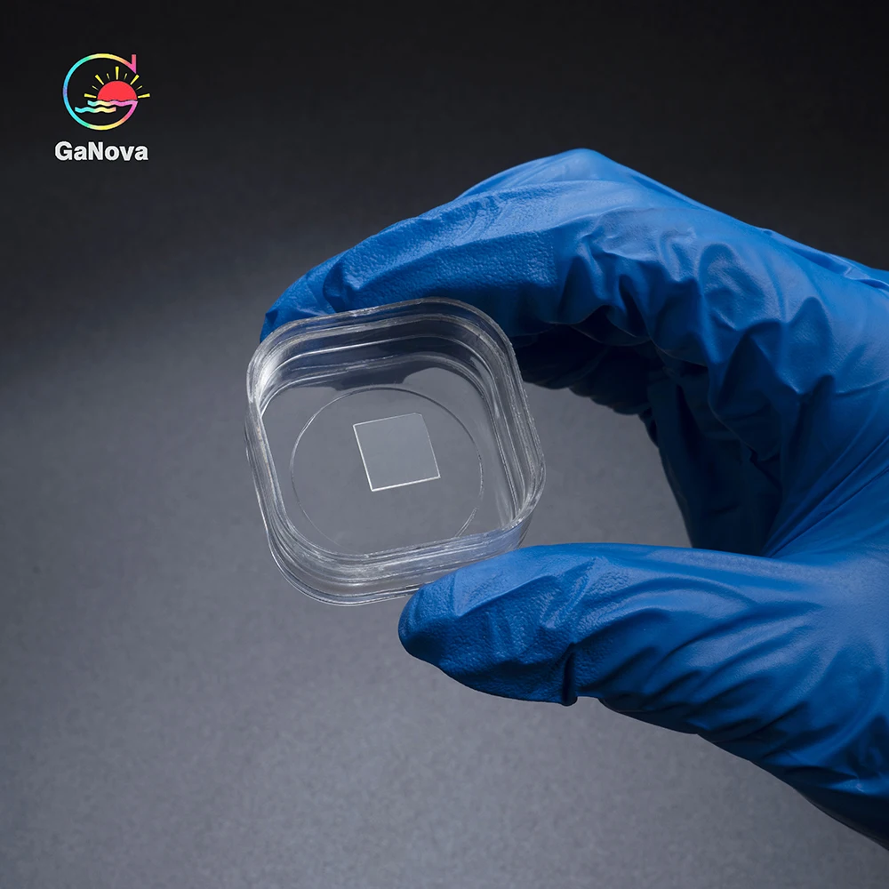
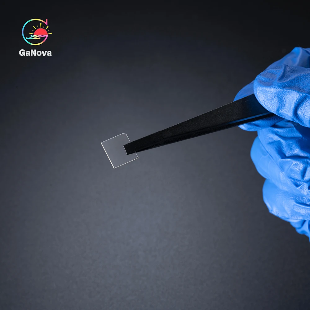
Автономная подложка GaN для силового устройства 10 0*10 5 кв. мм
- Категория: Semiconductors >>>
- Поставщик: Shanghai,Ganova,Electronic,Information,Co.,Ltd.
Поделиться:
Описание и отзывы
Трекер стоимости
| Месяц | Минимальная цена | Макс. стоимость |
|---|---|---|
| Sep-19-2025 | 255.71 $* | 268.76 $* |
| Aug-19-2025 | 253.50 $* | 266.83 $* |
| Jul-19-2025 | 212.4 $* | 223.1 $* |
| Jun-19-2025 | 248.88 $* | 260.88 $* |
| May-19-2025 | 216.63 $* | 227.88 $* |
| Apr-19-2025 | 244.94 $* | 256.12 $* |
| Mar-19-2025 | 242.15 $* | 254.51 $* |
| Feb-19-2025 | 240.38 $* | 252.86 $* |
| Jan-19-2025 | 238.30 $* | 250.69 $* |
Характеристики
Product Description

Specification
10 x 10.5 mm2 Free-standing GaN Substrates | ||||||
Item | GaN-FS-C-U-S10 | GaN-FS-C-N-S10 | GaN-FS-C-SI-S10 | |||
Dimensions | 10 x 10.5 mm² | |||||
Thickness | 350 ±25 µm | |||||
Orientation | C plane (0001) off angle toward M-axis 0.35 ±0.15° | |||||
Conduction Type | N-type | N-type | Semi-Insulating | |||
Resistivity(300K) | < 0.1 Ω·cm | < 0.05 Ω·cm | > 10⁶ Ω·cm | |||
TTV | ≤ 10 µm | |||||
BoW | - 10 µm ≤ BOW ≤ 10 µm | |||||
Ga Face Surface Roughness | < 0.2 nm (polished) or < 0.3 nm (polished and surface treatment for epitaxy) | |||||
N Face Surface Roughness | 0.5 ~1.5 μm option: 1~3 nm (fine ground); < 0.2 nm (polished) | |||||
Dislocation Density | From 1 x 10⁵to 3 x 10⁶ cm-² (calculated by CL)* | |||||
Macro Defect Density | 0 cm-² | |||||
Useable Area | > 90% (edge exclusion) | |||||
Package | Packaged in a class 100 clean room environment, in 6 PCS container, under a nitrogen atmosphere | |||||


Company Profile

Certifications

Exhibition

Packing & Delivery

FAQ

Q1: Are you trading company or manufacturer ?
We are factory.
Q2: How long is your delivery time?
Generally it is 3-5 days if the goods are in stock.or it is 7-10 days if the goods are not in stock, it is according to quantity.
Q3: Do you provide samples ? is it free or extra ?
We can provide samples free of charge according to the order quantity, but do not pay the freight.
Q4: What is your terms of payment ?
Payment <=5000USD, 100% in advance.
Paymen >=5000USD, 80% T/T in advance , balance before shippment.
Q5: How to guarantee the quality of your products?
Strict detection during production.Strict sampling inspection on products before shipment and intact product packaging ensured.

Похожие товары